Powered by Blogger.

Total Pageviews

I m on Twitter!

Sunday, March 25, 2012

THERMOCOUPLES: THE OPERATING PRINCIPLE


A thermocouple is a device made by two different wires joined at one end, called junction end or measuring end. The two wires are called thermoelements or legs of the thermocouple: the two thermoelements are distinguished as positive and negative ones. The other end of the thermocouple is called tail end or reference end. The junction end is immersed in the environment whose temperature T2 has to be measured, which can be for instance the temperature of a furnace at about 500°C, while the tail end is held at a different temperature T1, e.g. at ambient temperature.
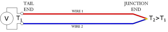
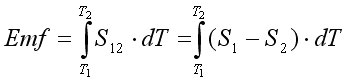


                                                                  Figure 1.


Because of the temperature difference between junction end and tail end a voltage difference can be measured between the two thermoelements at the tail end: so the thermocouple is a temperature-voltage transducer.


The temperature vs voltage relationship is given by:


                             Equation 1


Where Emf is the Electro-Motive Force or Voltage produced by the thermocople at the tail end, T1 and T2 are the temperatures of reference and measuring end respectively, S12 is called Seebeck coefficient of the thermocouple and S1 and S2 are the Seebeck coefficient of the two thermoelements; the Seebeck coefficient depends on the material the thermoelement is made of. Looking at Equation1 it can be noticed that:


  1. a null voltage is measured if the two thermoelements are made of the same materials: different materials are needed to make a temperature sensing device,

  2. a null voltage is measured if no temperature difference exists between the tail end and the junction end: a temperature difference is needed to operate the thermocouple,

  3. the Seebeck coefficient is temperature dependent.

In order to clarify the first point let us consider the following example (Figure2): when a temperature difference is applied between the two ends of a single Ni wire a voltage drop is developed across the wire itself. The end of the wire at the highest temperature, T2, is called hot end, while the end at the lowest temperature, T1, is called cold end.


 Voltage drop along one wire 
Figure2: Emf produced by a single wire


When a voltmeter, with Cu connection wires, is used to measure the voltage drop across the Ni wire, two junctions need to be made at the hot and cold ends between the Cu wire and the Ni wire; assuming that the voltmeter is at room temperature T1, one of the Cu wires of the voltmeter will experience along it the same temperature drop from T2 to T1 the Ni wire is experiencing. In the attempt to measure the voltage drop on the Ni wire a Ni-Cu thermocouple has been made and so the measured voltage is in reality the voltage drop along the Ni wire plus the voltage drop along the Cu wire.


The Emf along a single thermoelement cannot be measured: the Emf measured at the tail end in Figure1 is the sum of the voltage drop along each of the thermoelements. As two thermoelements are needed, the temperature measurement with thermocuoples is a differential measurement.


Note: if the wire in Figure2 was a Cu wire a null voltage would have been measured at the voltmeter. 


The temperature measurement with thermocouples is also a differential measurement because two different temperatures, T1 and T2, are involved. The desired temperature is the one at the junction end, T2. In order to have a useful transducer for measurement, a monotonic Emf versus junction end temperature T2 relationship is needed, so that for each temperature at the junction end a unique voltage is produced at the tail end.


However, from the integral in Equation1 it can be understood that the Emf depends on both T1 and T2: as T1 and T2 can change indipendently, a monotonic Emf vs T2 relationship cannot be defined if the tail end temperature is not constant. For this reason the tail end is mantained in an ice bath made by crushed ice and water in a Dewar flask: this produces a reference temperature of 0°C. All the voltage versus temperature relationships for thermocouples are referenced to 0°C.


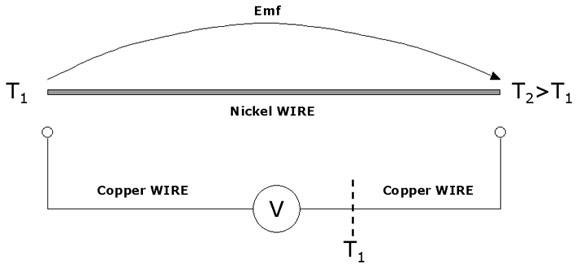
The resulting measuring system required for a thermocople is shown in Figure3.


 Thermocouple measuring system 
Figure3: A measuring system for thermocouples


In order to measure the voltage at the tail end, two copper wires are connected between the thermoelements and the voltmeter: both the Cu wires experience the same temperature difference and as a result the voltage drops along each of them are equal to each other and cancel out in the measurement at the voltmeter.


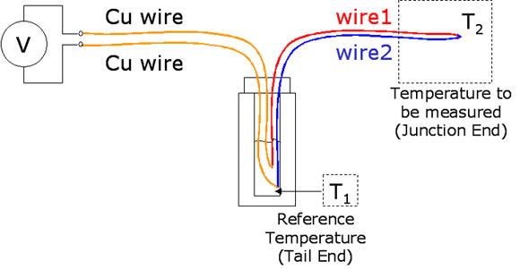
The ice bath is usually replaced in industrial application with an integrated circuit called cold junction compensator: in this case the tail end is at ambient temperature and the temperature fluctuations at the tail end are tolerated; in fact the cold junction compensator produces a voltage equal to the thermocouple voltage between 0°C and ambient temperature, which can be added to the voltage of the thermocouple at the tail end to reproduce the voltage versus temperature relationship of the thermocouple. 


A sketch of a thermocouple with cold junction compensation is reported in Figure4.


 COLD JUNCTION COMPENSATION 
Figure4: An example of Cold Junction Compensation


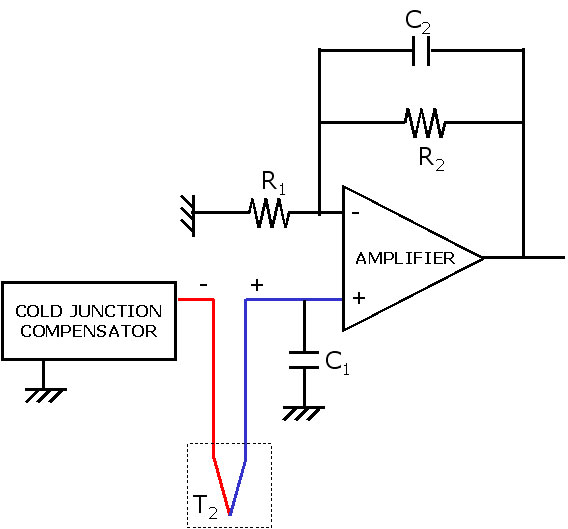
It should be underlined that the cold junction compensation cannot reproduce exactly the voltage versus temperature relationship of the thermocouple, but can only approximate it: for this reason the cold junction compensation introduces an error in the temperature measurement.


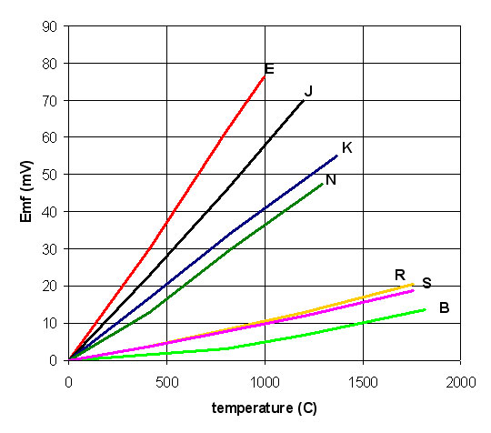
Figure4 shows also the filtering and amplification of the thermocouple. Being the thermocouple voltage a DC signal, removal of AC noise through filtering is beneficial; furthermore the thermocouples produce voltage of few tens of mV and for this reason amplification is required. The small voltage range for some of the most common thermocouples (letter designated thermocouples) is shown in Figure5, where their voltage versus temperature relationship is reported. 


Type R, S and B thermocouples use Pt-base thermoelements and they can operate at temperatures up to 1700°C; however they are more expensive and their voltage output is lower than type K and type N thermocouples, which use Ni-base thermoelements. However, Ni base thermocouples can operate at lower temperatures than the Pt-base ones. Table1 reports the approximate compositions for positive and negative thermoelements of the letter designated thermocouples.


 Emf vs Temperature for letter-designated thermocouples 
Figure5: Voltage vs Temperature relationship for letter-designated thermocouples 


Thermocouple typePositive ThermoelementNegative Thermoelement
BPt-30%RhPt-6%Rh
RPt-13%RhPt
SPt-10%RhPt
KNi-10%CrNi-5% other elements
NNi-14%Cr-1.5%SiNi-4.5%Si-0.1%Mg
ENi-10%Cr45%Ni-55%Cu
JFe45%Ni-55%Cu
Table1: Approximate composition for thermoelements of letter-designated thermocouples


All the voltage-temperature relationships of the letter designated thermocouples are monotonic, but not linear. For instance the type N thermocouple voltage output is defined by the following 10 degree polynomials, where t is the temperature in degree Celsius:
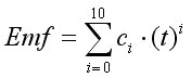


Type N polynomialEquation2


The coefficients Ci are reported in Table2.


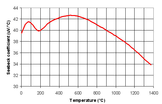
In order to have a linear voltage-temperature relationship the Seebeck coefficient should be constant with temperature (see Equation1); however the Seebeck coefficient is temperature dependent, as shown for instance for type K thermocouple in Figure6. Additional details on the voltage-temperature relatinships for letter designated thermocouple can be found at:


CoefficientTemperature range: (-270°C,0°C)Temperature range: (0°C,1300°C)
c0


0.000000000000 x100


0.000000000000 x100 
c1
0.261591059620 x10⁻¹

0.259293946010 x10⁻¹
c2
0.109574842280 x10⁻⁴

0.157101418800 x10⁻⁴
c3
-0.938411115540 x10⁻⁷

0.438256272370 x10⁻⁷
c4
-0.464120397590 x10⁻¹⁰

-0.252611697940 x10⁻⁹
c5
-0.263033577160 x10⁻¹¹

0.643118193390 x10⁻¹²
c6

-0.226534380030 x10⁻¹³

-0.100634715190 x10⁻¹⁴
c7

-0.760893007910 x10⁻¹⁶

0.997453389920 x10⁻¹⁸
c8

-0.934196678350 x10⁻¹⁹

-0.608632456070 x10⁻²¹
c9-
0.208492293390 x10⁻²⁴
c10-
-0.306821961510 x10⁻²⁸
Table2: Type N thermocouple coefficents      


 Type K Seebeck coefficient 
Figure6: Type K Seebeck coefficient vs Temperature

Virtual Oscilloscope using PIC Microcontroller


Virtual Oscilloscope using PIC Microcontroller


An oscilloscope is probably the most important instrument for observing and measuring electronic circuits. It allows you to observe timing, voltages, slopes, curves, and spikes of an electronic signal. A good digital oscilloscope can easily run you over $1000, but this scope will cost you a grand total of $40 for the kit, perhaps the cheapest scope you will ever buy.


Virtual Oscilloscope using PIC Microcontroller
Check out www.c-sharpcorner.com

Low pass filter for subwoofer


Many low pass filter circuits for subwoofer are given here and this is just another one. The circuit given here is based on the opamp TL062 from ST Micro electronics. TL062 is a dual high input impedance J-FET opamp which has very low power consumption and high slew rate. The opamp has excellent audio characteristics and is very suitable for this circuit.


Out of the two opamps inside TLC062, first one is wired as the mixer cum pre amplifier stage. The left and right channel are connected to the inverting input of IC1a for mixing. The gain of first stage can be adjusted using POT R3.The output of the first stage is connected to the input of second stage through the filter network comprising of components R5,R6,R7,R8,C4 and C5. The second opamp (IC1b) serves as a buffer and the filtered output is available at the pin 7 of the TLC062.


Circuit Diagram :


Power Suppy for Circuit :


Above Firgures Show How to make an Subwoffer Sound Producer.


Thanks :)))


Saturday, March 24, 2012

Fet Buffer for amplifiers


source: http://cappels.org/dproj/edfet/edfet.html

The EDFET drives like a FET, but with the bias stability of bipolar. Amps of output current can be controlled by milliamps of input current. The current gain is a design choice dictated by bandwidth. Two of things you have to consider when adding a power output stage to an op-amp circuit are the frequency response and the cross-over distortion in that stage.

This is especially true with wide band amplifiers, where the unity gain crossover needs to be at several hundred kilohertz. The stage is driven much the same as a complimentary pair output stage, but with the current gain that comes with using FETs., and with feedback within the output stage that that extends the buffer's bandwidth and regulates the quiescent current. More predictable operation allows the designer to design a circuit lower overall power dissipation and better closed loop stability.


Fet Buffer for amplifiers


The EDFET complimentary buffer is made up of a pair of unity gain buffers, one that drives in the positive direction and the other that drives in the negative direction. Pictured above is the positive driving half of the output stage.

Gain to make the output signal track the input signal comes from inverting transistor, Q1. The input signal is applied to the emitter of Q1 and the output of the amplifier is raised one diode drop to match the forward base-emitter drop of Q1, by diode connected transistor Q2. The buffer's offset is determined by the log of the magnitude of the mismatch in the emitter currents in Q1 and Q2, and it is directly proportional to the absolute temperature.

Since the saturation current usually isn't published for the transistors this expression is only usefully for appreciating the dependence of junction voltage on current and temperature. You can come up with your own value of I0 for a given transistor if you know all the other parameters and solve the above formula for I0. By the way, since, for most practical uses, you will be running at more than a thousand times the saturation current, the "+1" term can be dropped from practical calculations.

As an example, for the audio amplifier using a EDFET buffer shown in Figure 1. The following assumptions are applied: The maximum output voltage is 5 VDC with respect to ground, the power supply (VA) is 12 VDC, the maximum gate voltage is 8 VDC, the input capacitance, Ciss of the BUZ73 is 500 pf, and an...
http://cappels.org/dproj/edfet/edfet.html

Discrete Buffer: Diamond Buffer
Discrete Buffer: JISBOS Buffer

50 watts transistor amplifier


The amplifier and speakers that can handle medium-power is designed to provide a strictly amateur. Accidental overloads can damage the speakers, it is not appropriate for small systems.

What amp settings do not contain an element of the first connection wiring must be careful to work with.
Characteristics of the transistor, the fan or heat sink is cooled enough to find out if you need to focus!

Tech. parameters:
Power: + - 28V
Power: 50W / 4 ohms
Input sensitivity: 250mW of
Input resistance: 50 kOhm
Frequency range: 30Hz to - 30kHz

Optimal mobile recording portable player to another amplifier Multi Media.


Here, the schematics this power amplifier


List of components:
R1, R2, R9 - 56K
R3 - 3K3
R4, R6 - 100R
R5 - 220R
R7, R8 - 120R
R10 - 1K
R11 - 1R
C1 - in 1µF / 35V
C2 - 33P - Ceramics
C3 - the 100µF/35V
C4 - 100 N (220N) - Ceramic
C5, C6 - 4.7 UF / 35V
D1, D2 - 1N4007
T1, T2, T9 - BC546
Q3 - BC640
T4 - BD139
T5, T7 - BD711
T6 - BD140
T8 - BC639

Following the DC voltage amplifier and limiter speaker protection is needed.


Very Simply 10 Watts Stereo Power Amplifier-TDA2009A


Here are a power amplifier with TDA2009A integrated circuits produced by 10 +10 W stereo amplifier (see figure). As a result of ASIC, making her the production becomes very simple, the performance is not bad.

Her main performance characteristics in the table below.


Power Supply Voltage: DC 8-24V/1-2A
Power Output:


  1. 10W RMS / channel, 4 ohm load, 24V/DC power;
  2. 6W RMS / channel, 8 ohm load, 24V/DC power;
  3. 4W RMS / channel, 4 ohm load, 12V/DC power.

S/N: >75dB/10W output
Frequency response: 10Hz-50kHz,-3dB
Gain: 36dB
Input Level: 100mV Full output power

Schematic and Prototype:


Principle and production elements:


C1, C2 as the input capacitor, C10, C11 for the output capacitor. C6, C7 for the feedback capacitance. R1/R2, or (R3/R4) control the amount of feedback. Amplifier gain is equal to 1 + (R1/R2) = 68, or 37dB. C4, C5 for the power supply filter capacitor. The device maximum supply voltage of 28V. Hours of work required to add TDA2009A heat sink, and should pay attention to the power lines and then the choice of speaker wiring. Input should use shielded lines and as short as possible. Welding TDA200A not take too long when you pay attention, action to be fast, but if you want their full integration with the circuit board.

Tuesday, March 20, 2012

Transistor BC548

Datasheet :

BC548 is general purpose silicon, NPN, bipolar junction transistor. It is used for amplification and switching purposes. The current gain may vary between 110 and 800. The maximum DC current gain is 800.
 
Its equivalent transistors are 2N3904 and 2SC1815. These equivalent transistors however have different lead assignments. The variants of BC548 are 548A, 548B and 548C which vary in range of current gain and other characteristics.
 
The transistor terminals require a fixed DC voltage to operate in the desired region of its characteristic curves. This is known as the biasing. For amplification applications, the transistor is biased such that it is partly on for all input conditions. The input signal at base is amplified and taken at the emitter. BC548 is used in common emitter configuration for amplifiers. The voltage divider is the commonly used biasing mode. For switching applications, transistor is biased so that it remains fully on if there is a signal at its base. In the absence of base signal, it gets completely off.

Pin Diagram :

If You Like it, It will Just take few seconds to share it among your Friends !!!!

Monday, March 19, 2012

How comparator circuit works? Simple concepts in the study of comparator using opamp


Comparator is a circuit with two input terminals i.e. inverting and non-inverting. A standardimage voltage known as reference voltage Vref is connected to either inverting or non inverting terminal.
When it is connected to inverting terminal the input voltage Vin to compare is connected to non-inverting terminal or vice versa.
When the Vref = 0 and it is connected to inverting terminal, the circuit is called as INVERTING ZERO REFERENCE COMPARATOR. When it is connected to non-inverting terminal, the circuit is called as NON-INVERTING ZERO REFERENCE COMPARATOR.
When the Vref > 0 and it is connected to inverting terminal, the circuit is called as INVERTING NON-ZERO REFERENCE COMPARATOR. When it is connected to non-inverting terminal, the circuit is called as NON-INVERTING NON-ZERO REFERENCE COMPARATOR.
Whatever may be the input condition, the output of the comparator can have only three possible values i.e. output voltage Vo = +Vsat (Fully saturated positive voltage) or output voltage will be as such that it will beVo = –Vsat (Fully saturated negative voltage).
Now consider inverting zero reference comparator. For this the value ofVref = 0. The input voltage Vi is connected to non-inverting terminal. There are three possible conditions in this circuit, as follows –
When Vi > Vref, Vo = –Vsat
When Vi < Vref, Vo = +Vsat
When Vi = Vref, Vo = 0
Now consider inverting non-zero reference comparator. Let Vref = 3V. The input voltage Vi is connected to inverting terminal. There are three possible conditions in this circuit, as follows –
When Vi > Vref = 3V, Vo = –Vsat
When Vi < Vref = 3V, Vo = +Vsat
When Vi = Vref = 3V, Vo = 0
The above conditions occur because you are connecting higher i.e. positive voltage, which is greater than zero to inverting terminal. And the inverting terminal has the property to revert the polarity or sign of the voltage connected to it. So to understand the working of comparator just remember the property of inverting and non-inverting terminals of the operational amplifier.
image
Note: All these conditions will be exactly reversed and applicable to other circuit i.e. to the circuit of non-inverting zero reference comparator or the non-inverting non-zero reference comparator.

Saturday, March 17, 2012

Car stereo amplifier circuit using TDA2040

Given below is a car stereo amplifier circuit using  audio amplifier IC – TDA2040

Car Audio Amplifier Circuit:

Description of the circuit:

A car stereo amplifier circuit using TDA2040 is shown here. TDA2040 is a monolithic integrated audio amplifier that operates in Class AB mode. The IC has built in circuitry for short circuit protection and thermal shut down and more over it can be operated from a single supply too. The amplifier can deliver 12 watts into to a 8 ohm speaker.
In the circuit the IC is wired in order to operate from the cars 12V line. Capacitor C7 is the input DC decoupling capacitor and R4 provides feedback. Network consisting of resistor R5 and capacitor C5 provides high frequency stability and prevents any chance of oscillation. Capacitor C6 couples the ICs output to the speaker. C2 and C1 are power supply filters.

Circuit diagram of car stereo circuit using TDA2040


Notes:

  • Quality of the PCB is a very crucial factor in the amplifiers performance.
  • The amplifier can be operated from cars 12V line.
  • Heat sink is necessary for TDA2040.
  • All electrolytic capacitors must be rated 15V.
  • Only one channel is shown here. For stereo application you must make one more identical copy.

Wednesday, March 14, 2012

The Ways to Hack and Salvage The iPod Video LCD!

Electronics Hacks

You've a broken iPod, which has been leftover in the drawer for years but you just didn't know what you should do about it? Instead of abandoning it, why don't you take up some time and do something with it?
Basically, the 2.5" QVGA TFT LCD in the iPod video is very valuable and it can be salvaged then use in the large-scale project! For this purpose, you should make sure that you're using the iPod, which its hard disk was permanently dead (Well, if you're wealthy enough, then go ahead and use the brand new iPod Nano!).
The first problem that you might be faced in this project will be the connector, where its actually a 0.3 mm pitch FFC, and this will cause a fiddle to connect with. Since the connector is staggered altogether, with those pins on alternate sides, therefore the wires that are soldered on to it are 0.6 mm apart. Your task here is to keep them look tidily and flat, also to stop them fouling the flex cable entry and locking lever as well!
This project will take more time than you thought here, so the patient is the main key, if you want to involve yourself in it! [source]

Saturday, March 3, 2012

KEIL MICROVISION 4 FULL VERSION FREE DOWNLOAD | Mediafire Link

Keil was founded in 1986 to market add-on products for the development tools provided by many of the silicon vendors. Keil implemented the first C compiler designed from the ground-up specifically for the 8051 micro controller.


Keil provides a broad range of development tools like ANSI C compiler, macro assemblers, debuggers and simulators, linkers, IDE, library managers, real-time operating systems and evaluation boards for 8051, 251, ARM, and XC16x/C16x/ST10 families.


Keil Tutorial  Video:
I Have Given Simple Tutorial on Keil.....


(all links are mediafire links )


or
 copy paste below link in ur browser


http://www.mediafire.com/?auqhnfr0fd4jpq1


Wednesday, February 29, 2012

FM radio controlled anti-theft alarm

This FM radio-controlled anti- theft alarm can be used with any vehicle having 6- to 12-volt DC supply system. The mini VHF, FM transmitter is fitted in the vehicle at night when it is parked in the car porch or car park. The receiver unit with CXA1019, a single IC-based FM radio module, which is freely available in the market at reasonable rate, is kept inside. Receiver is tuned to the transmitter’s frequency.
When the transmitter is on and the signals are being received by FM radio receiver, no hissing noise is available at the output of receiver. Thus transistor T2 (BC548) does not conduct. This results in the relay driver transistor T3 getting its forward base bias via 10k resistor R5 and the relay gets energized.
When an intruder tries to drive the car and takes it a few meters away from the car porch, the radio link between the car (transmitter) and alarm (receiver) is broken. As a result FM radio module gene-rates hissing noise.
Hissing AC signals are coupled to relay switching circuit via audio transformer. These AC signals are rectified and filtered by diode D1 and capacitor C8, and the resulting positive DC voltage provides a forward bias to transistor T2. Thus transistor T2 conducts, and it pulls the base of relay driver transistor T3 to ground level.
The relay thus gets de-activated and the alarm connected via N/C contacts of relay is switched on. If, by chance, the intruder finds out about the wireless alarm and disconnects the transmitter from battery, still remote alarm remains activated because in the absence of signal, the receiver continues to produce hissing noise at its output. So the burglar alarm is fool-proof and highly reliable.

Fundamentals of resistors

Detailed information about resistors…

Resistor the resistor is an element which opposes to the flow of electric current. Resistance is theres property of the material by which it opposes to the flow of current, the current may be either AC or DC; it offers equal resistance to both. Basically their are two types of resistors : fixed and variable resistors. The fixed resistors have a given fixed value. It does not change by any physical means. A fixed resistor has a specific value printed on its body, either in the form of color codes or in numerical. The general symbols of a fixed resistor is given here. Any fixed resistor is always denoted by “R” and if there are more than one resistors then they are shown as R1, R2, R3 . . . . and so on. Variable resistor has a variable value over a fixed range. Its resistance can be changed by adjusting the knob attached to the shaft of the variable resistor. A variable resistor is also subdivided into four main types : all these types have the same function, only size and shape differs. Symbols of fixed and variable resistor are given below.dsv
The unit of resistance is the ohm, and the chief parameter for any resistor is its resistance. However there are a number of other parameters that are also important. In view of these other resistor parameters there are several different resistor types that are available. In fact choosing the right type of resistor for a given application can be important. Although many resistors will work in a variety of applications the type of resistor can be important in some cases. Accordingly it is necessary to know about the different resistor types, and in which applications each type of resistor can be used.

Basic distinction of resistor types

The first major categories into which the different types of resistor can be fitted is into whether they are fixed or variable. These different resistor types are used for different applications:
  • Fixed resistors:   Fixed resistors are by far the most widely used type of resistor. They are used in electronics circuits to set the right conditions in a circuit. Their values are determined during the design phase of the circuit, and they should never need to be changed to "adjust" the circuit. There are many different types of resistor which can be used in different circumstances and these different types of resistor are described in further detail below.
  • Variable resistors:   These resistors consist of a fixed resistor element and a slider which taps onto the main resistor element. This gives three connections to the component: two connected to the fixed element, and the third is the slider. In this way the component acts as a variable potential divider if all three connections are used. It is possible to connect to the slider and one end to provide a resistor with variable resistance. Further details of variable resistor can be found on the variable resistors page accessible through the "Related Articles" list which can be found on the left hand side of this page below the main menu.

Fixed resistor types

There are a number of different types of fixed resistor:
  • Carbon composition:   These types were once very common, but are now seldom used. They are formed by mixing carbon granules with a binder which was then made into a small rod. This type of resistor was large by today’s standards and suffered from a large negative temperature coefficient. The resistors also suffered from a large and erratic irreversible changes in resistance as a result of heat or age. In addition to this the granular nature of the carbon and binder lead to high levels of noise being generated when current flowed.
  • Carbon film:   This resistor type is formed by "cracking" a hydrocarbon onto a ceramic former. The resulting deposited film had its resistance set by cutting a helix into the film. This made these resistors highly inductive and of little use for many RF applications. They exhibited a temperature coefficient of between -100 and -900 parts per million per degree Celcius. The carbon film is protected either by a conformal epoxy coating or a ceramic tube.
  • Metal oxide:   This type of resistor is now the most widely used form of resistor. Rather than using a carbon film, this resistor type uses a metal oxide film deposited on a ceramic rod. As with the carbon film, the the resistance can be adjusted by cutting a helical grove in the film. Again the film is protected using a conformal epoxy coating. This type of resistor has a temperature coefficient of around + or – 15 parts per million per degree Celcius, giving it a far superior performance tot hat of any carbon based resistor. Additionally this type of resistor can be supplied to a much closer tolerance, 5% or even 2% being standard, with 1% versions available. They also exhibit a much lower noise level than carbon types of resistor.
  • Wire wound:   This resistor type is generally reserved for high power applications. These resistors are made by winding wire with a higher than normal resistance (resistance wire) on a former. The more expensive varieties are wound on a ceramic former and they may be covered by a vitreous or silicone enamel. This resistor type is suited to high powers and exhibits a high level of reliability at high powers along with a comparatively low level of temperature coefficient, although this will depend on a number of factors including the former, wire used, etc.
Classification of variable resistors they are the variable resistors made up of carbon or wire wound type material. They are especially used for controlling voltage and current in the circuit. According to the quality they are useful for industrial, commercial and military grades circuits. There are also some modern types of variable resistors, which are known as ganged type (often called as tandem type also). They are in pairs which are connected internally to vary the values at a time. It is the most popular type of resistor. It is widely used in the control of volume, bass, treble brightness and contrast controls of tape recorders and TV sets. It has three terminals and its
resistance is fixed between the two outer terminals. The middle terminal is known as the wiper. Between the two adjacent points the resistance can be changed by turning the position of the shaft. This shaft can be attached to a control knob for convenience. It is made-up of carbon material and it has two main types : the linear type and logarithmic type. In linear type [known as LIN] the resistance changes linearly and uniformly. However in logarithmic type [known as LOG] the resistance changes on a log scale. Generally the LIN type resistors are used for controlling of volume and treble. In the control of bass, brightness and contrast the LOG types are used. In general the classification of potentiometers is as follows –

dsv


Classification of Potentiometers
image
Rheostat is an important device, in the high voltage and high current adjustments. They are made up of resistive wires like Nichrome, Tungsten and such high resistive materials. It has three terminals – the two end terminals are the end points of the complete wire and the middle terminals is connected to the wiper which is rested tightly on the naked portion of the wire. Its internal resistance, is decided by the length of the wire used. The basic disadvantage of this device over carbon variable resistor is that it has Ohmic resistance as well as inductive reactance (XL), since the resistive wire is wound in coil fashion. Hence it is not suitable where high frequency current is to be controlled. It is therefore specially used for limiting DC current.

Saturday, February 25, 2012

Log amplifier

Log amplifier is a linear circuit in which the output voltage will be a constant times the natural logarithm of the input. The basic output equation of a log amplifier is v Vout = K ln (Vin/Vref); where Vref is the constant of normalisation, and K is the scale factor. Log amplifier finds a lot of application in electronic fields like multiplication or division (they can be performed by the addition and subtraction of the logs of the operand), signal processing, computerised process control, compression, decompression, RMS value detection etc. Basically there are two log amp configurations: Opamp-diode log amplifier and Opamp-transistor log.

Opamp-diode log amplifier.

diode opamp log amplifier
Opamp-diode log amplifier
The schematic of a simple Opamp-diode log amplifier is shown above. This is nothing but an opamp wired in closed loop inverting configuration with a diode in the feedback path. The voltage across the diode will be always proportional to the log of the current through it and when a diode is placed in the feedback path of an opamp in inverting mode, the output voltage will be proportional to the negative log of the input current. Since the input current is proportional to the input voltage, we can say that the output voltage will be proportional to the negative log of the input voltage.
According to the PN junction diode equation, the relationship between current and voltage for a diode is
Id = Is (e(Vd/Vt)-1)…………(1)
Where Id is the diode current, Is is the saturation current, Vd is the voltage across the diode and Vt is the thermal voltage.
Since Vd the voltage across the diode is positive here and Vt the thermal voltage is a small quantity, the equation (1) can be approximated as
Id = Is e(Vd/Vt)…………………(2)
Since an ideal opamp has infinite input resistance, the input current Ir has only one path, that is through the diode. That means the input current is equal to the diode current Id.
=> Ir = Id ………………….(3)
Since the inverting input pin of the opamp is virtually grounded, we can say that
Ir = Vin/R
Since Ir = Id (from equation (3) )
Vin/R = Id …………………..(4)
Comparing equation (4) and (2) we have
Vin/R = Is e(Vd/Vt)
i.e. Vin = Is R e(Vd/Vt)……………(5)
Considering that the negative of the voltage across diode is the output voltage Vout (see the circuit diagram (fig1)), we can rearrange the equation (5) to get
Vout = -Vt In(Vin/IsR)

Opamp transistor log amplifier.

In this configuration a transistor is placed in the feedback path of an opamp wired in inverting mode. Collector of the transistor is connected to the inverting input of the opamp, emitter to output and base is grounded. The necessary condition for a log amp to work is that the input voltage must be always positive. Circuit diagram of an Opamp-transistor log amplifier is shown below.
transistor-opamp log amplifier
Opamp-transistor log amplifier
From  Fig 2  it is clear that base-emitter voltage of the transistor Vbe = -Vout  ………(1)
We know that Ic = Iso (e(Vbe/Vt)-1) ………….(2)
Where Ic is the collector current of the transistor, Iso the saturation current, Vbe the base emitter voltage and Vt the thermal voltage.
Equation (1) can be approximated as Ic = Iso e(Vbe/Vt) ………….(3)
Ie, Vbe = Vt In (Ic/Iso) …………….(4)
Since input pin of an ideal opamp has infinite input impedance, the only path for the input current Ir is through the transistor and that means Ir = Ic.
Since the inverting input of the opamp is virtually grounded
Ir = Vin/R
That means Ic = Vin/R  ……………(5)
From equations (5) , (4) and (1) it is clear that
Vout = -Vt ln (Vin/IsoR1)………….(6)

Ads By Sponsers